Universal PCB with bus lines
As I was working on my computer I started on breadboards. It worked fine until I wanted some RAM and I just ran out of jumper cables. So I thought I need some proper PCBs. The problem is - if you order something from PCB manufacturer it will be at least 5 of given type. Here I needed every board to be different. I checked readily available prototype PCBs and all would require much of work to greate buses and route all chips to them. So the goal is - create a PCB that is generic enough but yet removes as much of the work as possible.
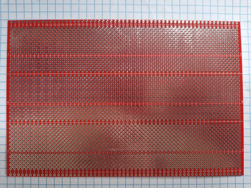
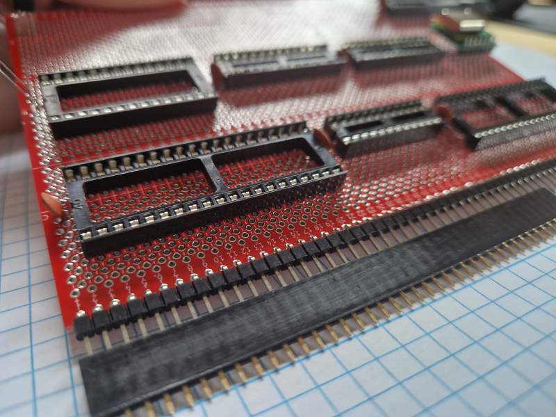
I thought to route bus between ICs legs so they could run the entire height of the board. DIP legs are 2.54mm apart (0.1”) so I needed holes 1.27mm apart - one set for bus and second set for ICs. Evenly distributed on 10x15 cm board was over 8000 holes. Also the holes need to be at least 0.8mm in diameter to fit in pin headers. This gave very little room for soldering pad but I squized it in… PCB manufacturer complainde for the number of holes and trace spacing :( and wanted to charge extra.
So I did the 2nd attempt - I removed every 2nd hole on the buses and every 2nd hole on chip traces and shifted them vertically 1.27mm. This got accepted. Manufacturer kindly suggested gold plating (soooo expensive) but agreed to go with HASL noting the quality may be worse than usual. But the boards look great and the cost of making 10 is not different than buying 10 proto PCBs of this size. I made them 1mm thick for a test - they are rigid enough.
The design:
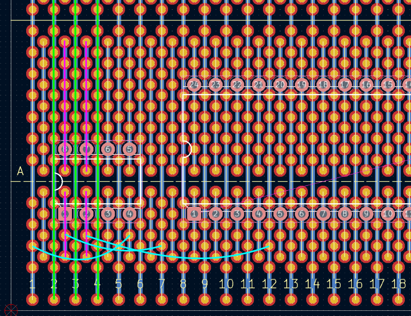 Buses are numbered from 1 to 58 - I marked few of them in green.
There are 3 rows of ICs A, B and C which have short traces reaching PCB legs - marked in magenta. To connect ICs to buses and power you only need mostly horizontal connections - cyan.
The same board can be used as a backplane and as a card. You can connect boards in one after another in a flat arrangement 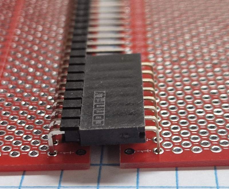
or perpendicular (as a backplane and cards) 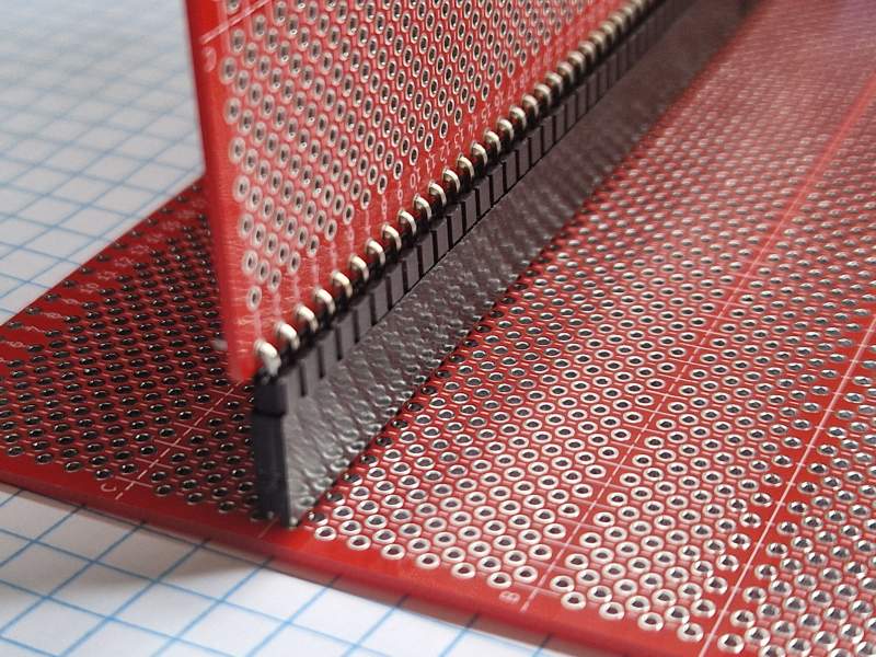
And an example of how ICs could be placed on the board:
References:
- The project: GitHub